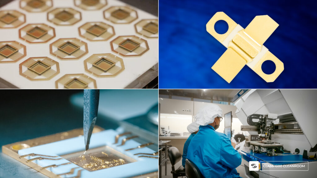
StratEdge offers post-fired ceramic and lower-cost molded ceramic packages. The company’s ISO 9001:2015 certified facility features a Class 1000 cleanroom with Class 100 work areas for performing sensitive microelectronic assembly. (Image courtesy StratEdge)
SANTEE, Calif.—A company in the greater San Diego metropolitan area is working to redefine the landscape of semiconductor packaging with its cutting-edge molded and post-fired ceramic packages, supported by high-reliability assembly services.
StratEdge Corporation offers post-fired ceramic and lower-cost molded ceramic packages, specializing in packages for the extreme demands of gallium arsenide (GaAs) and gallium nitride (GaN) devices. The company designs, manufactures, and provides assembly services for high-frequency and high-power semiconductor packages operating from DC to 63+ GHz, according to a release from StratEdge.
“We manufacture our high-frequency packages with precision, using post-fired ceramics with laser-cut features to control tight tolerances, thermally-enhanced metal bases that dissipate heat, and electrical transition designs that provide exceptionally low electrical losses,” said StratEdge Vice President of Global Sales Casey Krawiec, in the release.
StratEdge’s molded ceramic packages reportedly offer excellent reliability and are designed to handle high-frequency chips up to 18 GHz. With more than 200 standard outlines available, they provide a vast array of packaging options, the company said in the release.
Complementing the molded ceramic packages, StratEdge’s post-fired ceramic packages are said to excel in thermal management for compound semiconductors like GaN, GaAs, and SiC, operating from DC to 63+ GHz.
“The packages provide ultra-low loss performance over a wide range of frequencies, depending on the style and mounting configuration,” the release said. “Many open-tooled designs are available with 50 ohm impedance high-frequency transitions, which provide convenience and ease for packaging high-performance semiconductors.”
StratEdge’s quality management system is ISO 9001:2015 certified for the design and manufacture of semiconductor packages, filters, and electronic component assembly, according to its management system certificate. The company’s facility features a Class 1000 cleanroom with Class 100 work areas for performing sensitive microelectronic assembly. It’s equipped with state-of-the-art assembly equipment, including a device bonder with a eutectic gold-tin (AuSn) attachment station that is reported to achieve bond line thicknesses of 6µm. This refined eutectic die attach technology maximizes power output for GaN devices, resulting in lower junction temperatures and increased device reliability, the company said.
“Working with compound semiconductors, such as GaN, requires a package that can best dissipate the heat from the device while ensuring optimal performance,” Krawiec added. “Although the package plays the most critical part, the way the chip is attached can also make a significant difference in the device’s performance.”
Engineered to meet the rigorous demands of modern applications, the StratEdge molded and post-fired ceramic packages are tailored for markets that include telecom, wireless, satellite, and defense, among others.
