Illustration by Alex Davis and Alex Cabrera/ASU
Arizona State University is plugged into this next breakthrough in microchip tech with curriculum, partnerships with industry leaders
By Mary Beth Faller
Microchips are hot.
The tiny bits of silicon are integral to 21st-century life because they power the smartphones we rely on, the cars we drive and the advanced weaponry that is the backbone of national security. They’re so important that the disruption of the microchip supply chain during the pandemic became an urgent national security issue.
Also, microchips are literally hot.
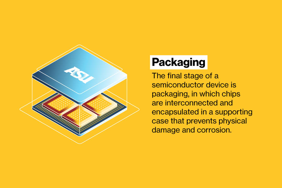
Those tiny chips have mighty computing power, which builds up heat around the microchip. From the beginning, in the 1950s, manufacturers designed packaging—the materials around the chips—to mitigate heat, provide protection and enable electrical current to flow.
Over the decades, as the chips became more powerful, the packaging became more sophisticated.
Now, “advanced packaging” is a critical part of the design and manufacture of chips, not only to protect them from the heat generated by ever-increasing power but also as a way to actually improve their performance—critical as the strategy of adding more transistors on ever smaller chips, the practice that has driven the industry since the 1960s, reaches both its financial and physical limits.
The newest generation of advanced packaging is integrated with the chips during the manufacturing process to make them work faster and even combine different kinds of chips onto one wafer for super advanced capabilities like artificial intelligence.
It’s as if you had a glove that not only protected your hand but also made it stronger.
Arizona State University is poised to be a major player in this next breakthrough in microchip technology. The university is one of the few in the country that is teaching advanced packaging to its students, creating the skilled workforce that’s desperately needed by the semiconductor industry. A key asset in doing that is ASU’s partnerships with industry leaders to research the next innovations as well as create a cutting-edge production line.
ASU has launched a ground-breaking collaboration with Deca Technologies, a Tempe, Arizona-based provider of advanced packaging technology. ASU and Deca will create North America’s first fan-out wafer-level packaging research and development center. The new Center for Advanced Wafer-Level Packaging Applications and Development will expand domestic semiconductor manufacturing and drive advancements in artificial intelligence, machine learning, automotive electronics and high-performance computing.
In addition, ASU recently entered into a partnership with NXP Semiconductors focused on advanced packaging. Fueled by the support of the Arizona Commerce Authority, ASU received $17.5 million to expand research, development and workforce training.
It’s all part of a strategy launched several years ago by ASU to become a leader in the field of advanced packaging, according to Zachary Holman, a professor in the School of Electrical, Computer and Energy Engineering at ASU.
“ASU’s competitive advantage in advanced packaging stems from our scale, the innovativeness of our faculty and our partnerships, which extend both locally with companies like Deca Technologies, NXP and others, and farther afield,” he said.
“Advanced packaging will allow the semiconductor industry to keep growing, even though shrinking transistors is no longer the path forward. And here in Arizona we have an excellent advanced packaging industry, and it’s growing.”
The COVID-19 pandemic highlighted America’s dependency on Asia when supply chain disruptions led to critical shortages impacting consumer purchases of everything from computers to automobiles to home appliances.
In 2022, the bipartisan CHIPS and Science Act was signed into law, releasing $52 billion over five years to help the U.S. regain its superiority in semiconductor research, manufacturing and supply chain logistics.
ASU’s role in helping the U.S. become a leader in advanced packaging will enable a secure supply chain, said Holman, who also is vice dean for research and innovation in the Ira A. Fulton Schools of Engineering at ASU.
“A secure supply chain allows us to make the electronics that we need for everything from consumer products to vehicles to weapons for the defense industry,” he said.

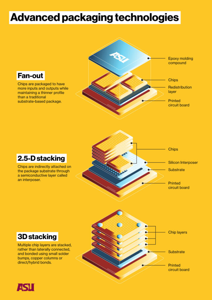
Different types of packaging are used for different applications. Illustration by Alex Davis and Alex Cabrera/ASU
Making chips do new tricks
Historically, electronics got better by making transistors smaller.
That’s a function of Moore’s Law, a 1965 prediction by Gordon Moore, co-founder of Intel, who said that the number of transistors on microchips would double every two years, increasing computing power while decreasing costs.
But Moore’s Law is no more, Holman said.
“We’ve reached a fundamental limit where we can’t make things better just by making transistors smaller anymore. And so we have to come up with a new way,” he said.
Advanced packaging was developed around 2000.
“Advanced packaging allows us to put chips together in new ways to achieve new functionalities, to speed up electronics, to make them do new tricks without making transistors smaller,” Holman said.
Different types of packaging are used for different applications. A smartphone combines different packaging for the graphics, the user interface and the power management. An autonomous vehicle that uses artificial intelligence is even more complex.
Tim Olson founded Deca Technologies in 2009, after leading research and development at semiconductor company Amkor.
“I had a passion to transform the way advanced packaging was done, and I felt we could do it a better way,” he said.
Deca Technologies specializes in a process called fan-out wafer-level packaging and provides components used in iPhones.
“Fan-out wafer-level packaging is very unique and, at a highest order, the fan-out part of it is ‘glue.’ So view fan-out as glue, and you glue together things that you want to put together, whether that’s a processor chip, a memory chip, a combination of memory chips, an RF (radio frequency) communication chip, a battery—whatever it is that you want to put together,” Olson said.
“There’s really no other packaging technology like it where you can glue those things together laterally, vertically, in any directions and orientations that you want.”
Even as advanced packaging technology has surged in the past several years, there’s still a long way to go, Olson said.
“Advanced packaging today, for all the buzz that we hear, is really in its infancy,” he said.
“Over the next decade, there will be orders of magnitude scaling required in advanced packaging to keep up with the demands of artificial intelligence, the real-time nature of autonomous vehicles and things like that.”
The new ASU-Deca Technologies collaboration—the Center for Advanced Wafer-Level Packaging Applications and Development—will be in the MacroTechnology Works facility in ASU’s Research Park in Tempe. MacroTechnology Works is a former Motorola semiconductor fabrication facility that ASU bought in 2004. It’s more than 250,000 square feet with more than 40,000 square feet of “clean room” space.
“This center will allow ASU and Deca to have a joint place, a set of tools, capabilities and people to further develop what is possible in packaging, as well as training the next generation workforce by having ASU students use the equipment in the center,” Holman said.
More than 20 new pieces of equipment will power the production line.
Olson said the new center will develop many types of solutions.
“It’s really the first fab in the U.S. where you have an open innovation platform where folks can come together, like students or industry users, producers, equipment companies, material companies, and work together on a foundation of technology that’s being provided by Deca and integrated by ASU,” he said.
Olson is excited for Deca Technologies’ work with students.
“The amazing advantage of students is their intellectual curiosity,” he said.
“When they’re working on a problem or working on a project and they see something that doesn’t quite work the way we’d like it to work, they ask enough questions and they dig into it enough to often create a better way to do it or to solve a fundamental problem that’s been hampering the technology for a long time.”
Building a semiconductor workforce
As part of its strategy to become a leader in advanced packaging, ASU started hiring experts to become faculty. One of them is Leslie Hwang, assistant professor in the School of Electrical, Computer and Energy Engineering, who creates software models that predict chip reliability.
“Packaging has become a more critical issue as technology is scaling,” she said.
“We’re trying to pack so much power and so much function into smaller domains that thermal issues are becoming critical. There’s not enough area (for heat) to dissipate.
“For a chip to function, you need a maximum temperature of 87 degrees or the chips are being fried, and you definitely don’t want that. A higher temperature means slower function and accelerated aging and mechanical stress—warping the material.”
Hwang uses machine learning to create computer models that analyze multiple, simultaneous factors—such as temperature and mechanical stress during manufacturing—to determine chip reliability.
“You need to predict the actual usage as much as possible in advance to do that,” she said.
“If you can predict well, you’re not only saving cost, but it can be a foundation to build a better design. And by coming up with more effective packaging techniques, we can actually elongate the lifetime of the electronic from the consumer side.”
ASU is one of the few universities in the country that’s teaching advanced packaging in its engineering curriculum, with a focus on the interdisciplinary nature of the industry.
“Here at ASU, we currently have 200 students-plus doing packaging-related courses,” said Chris Bailey, professor in the School of Electrical, Computer and Energy Engineering.
“We’re seeing significant growth in those student numbers, but also we are engaging with the wider community and looking at different activities to ensure we have the workforce for the future.”
Bailey teaches a graduate course on the fundamentals of packaging, from the 1960s to today.
“And this is one of the great things about ASU—I have students there from chemical engineering, from materials science, from electrical engineering and from mechanical engineering because they’re all important for advanced semiconductor packaging,” he said.
He also teaches a course on design and modeling for advanced packaging.
“So they’re sitting in front of computers doing electronic (computer-assisted design), they’re undertaking thermal calculations, electromagnetic calculations, the mechanical calculations. But they also learn the need to understand metrology and materials behavior.
“And that’s where we need that multidisciplinary knowledge for the students, and also for the next generation of advanced semiconductor packaging engineers.”
Bailey said that industry partnerships teach students the real-world challenges of manufacturing.
“We’re engaging with companies to ask, ‘What if we do it this way?’” he said.
While designing and manufacturing microelectronics to be more powerful and efficient is a key to America’s advancement, ASU is also helping to solve the critical problem of producing the workforce to do it.
“With all the buzz you hear about chips and semiconductors, with TSMC coming to town, with Intel, and with the $8 billion announced recently from the U.S. government and all the things happening in the Valley.… it’s still incredibly difficult for us to find the right talent,” Olson said.
“So, I think what this partnership brings is the ability to create a very significantly enhanced pool of talent for not only for our business, but for all the businesses related to the semiconductor industry.”
Sally Morton, executive vice president of ASU’s Knowledge Enterprise, sees the role of the university as a strength both locally and nationally.
“Arizona State University is advancing the local semiconductor industry and positioning our state as a leader in semiconductor research, manufacturing and job growth,” Morton said. “With help from our industry partners, we are bridging the gap between lab to fab with advanced and innovative packaging solutions to scale up production methods and optimize efficiency and cost-effectiveness.
“This will strengthen domestic production and the nation’s critical supply chain, while enhancing the U.S.’s competitiveness in the global semiconductor market in areas such as electronics, telecommunications and defense.”
Mary Beth Faller is a writer for ASU News.
This article originally appeared in ASU News. Republished with permission of Arizona State University.
Source:
https://news.asu.edu/20240419-science-and-technology-advanced-packaging-next-big-thing-semiconductors
