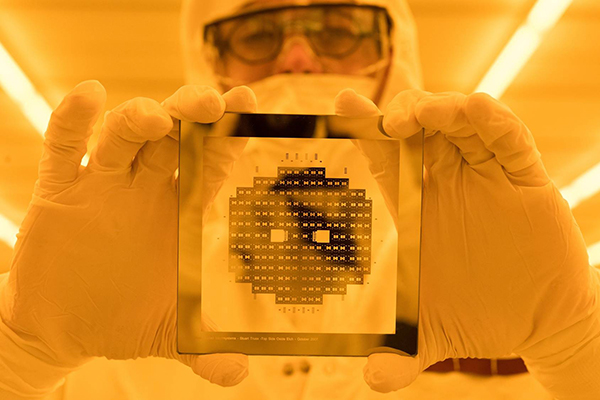
A Georgia Tech researcher holding an etched wafer. (Photo courtesy Christopher McKenney and Rob Felt)
Smartphones. Kettles. MRI machines. LED lightbulbs. Cars. Almost every electronic device uses a semiconductor, a tiny silicon chip made of myriad transistors that can perform billions of computations in a second.
By Tess Malone
ATLANTA—Semiconductors make our world run, but the industry faces a turning point.
For decades, computer chip efficiency has doubled every two years, but that progress is slowing. To complicate the problem further, global demand for semiconductors threatens to outpace the supply. The U.S. has the opportunity to meet the growing need for chips—both by increasing domestic manufacturing and building up the workforce, which is at its lowest in decades. To bolster semiconductor research and manufacturing, in 2022, Congress passed the $52.7 billion bipartisan CHIPS and Science Act that President Joe Biden signed into law. New paradigms and pioneers are needed to make these critical advances.
Georgia Tech is playing a significant role in creating the next generation of chips, as the Institute is especially well positioned to innovate in the semiconductor field. All areas of the semiconductor stack—the components that build a chip, from hardware to artificial intelligence—are studied at Tech, and collaboration among faculty is a hallmark of its research enterprise. Such cooperation is necessary to build better chips, since they need to be reinvented in every layer of the stack.
“Because of our depth and breadth in all of these areas, Georgia Tech has enormous strength,” said Michael Filler, interim executive director of the Institute for Electronics and Nanotechnology. “That’s why we’re set up to help push the industry—and the country—forward.”
The innovation doesn’t stop with research, though. Georgia Tech is also growing the industry’s workforce. From summer camps for middle schoolers to teaching undergraduates how to use a cleanroom, Georgia Tech trains the people who will build the semiconductors of the future. Industry partnerships enable students to work on crucial real-world issues and find work in the field immediately. The Institute is also ensuring that the research expands far past the borders of campus by developing collaborations and mentorship with researchers at minority-serving institutions.
Explaining the Semiconductor Slowdown
Since the 1950s, the number of transistors able to fit on a computer chip has doubled almost every two years, a concept known as Moore’s Law. However, this progress is lagging. To continue to innovate the current chip design takes considerable money and electrical power. The industry infrastructure to build these chips is also currently too weak to meet demand.
“We can keep making advances, but at what cost?” Filler said. “We struggle with fragile supply chains and constant security vulnerabilities.”
Since semiconductors are used in transportation, the military, and industry, security issues entail more than a manufacturing problem. “It’s not just a matter of economic security,” said George White, senior director of strategic partnerships for Research. White has worked in semiconductor research for 30 years. “It’s also a matter of national security.”
Georgia Tech researchers believe the key to pushing the field of semiconductors forward is creating a whole new type of chip. They can imagine these new, better chips designed in different layouts and with new materials. (Photo courtesy Christopher McKenney and Rob Felt)
Currently, the U.S. manufactures just 12% of the global semiconductor supply. The country now has a chance to help create a better chip—and, in the process, develop a new industry that employs millions of Americans.
Georgia Tech researchers believe the key to pushing the field forward is creating a whole new type of chip. They can imagine these new, better chips designed in different layouts and with new materials.
Currently, the U.S. manufactures just 12 percent of the global semiconductor supply. The country now has a chance to help create a better chip—and, in the process, develop a new industry that employs millions of Americans.
Researching Up and Down the Semiconductor Stack
Chip innovation happens at all levels: designing and building the circuits, creating applications for chips, and developing the chip’s packaging. Georgia Tech researchers work in each of these areas.
Professor Saibal Mukhopadhyay in the School of Electrical and Computer Engineering (ECE) directs CogniSense: Center on Cognitive Multispectral Sensors, which works on innovations in the semiconductor space.
Similarly, Arijit Raychowdhury, ECE chair, directs the Center for the Co-Design of Cognitive Systems (CoCoSys), where his team plan to leverage chip design to strengthen AI capabilities and, eventually, build a humanlike interface capable of using the same five senses and intelligence humans do. “We want to innovate on the next generation of algorithms and hardware, to make AI more data- and hardware-efficient, as well as make AI models more transparent and comprehensible,” Raychowdhury said.
ECE’s Callie Hao, an assistant professor, works in three areas of the semiconductor stack’s architectural level: optimizing machine learning to be more efficient on hardware, customizing hardware to run algorithms faster, and creating automation tools for hardware design. “We design the architecture or build the tools to facilitate the architecture design process,” she said. “We work on the layer above semiconductors so architects can better use the cutting-edge semiconductor technologies.”
Researchers in the College of Computing develop AI models optimized for efficient hardware execution. Celine Lin, an associate professor in the School of Computer Science, focuses on accelerating the development of efficient AI solutions. “My team and I are dedicated to enhancing the energy efficiency of AI solutions to optimize semiconductor usage while leveraging the powerful capabilities of AI models to expedite the development of semiconductor advancements,” she explained.
Finally, advanced packaging pulls together different chips into a single, coherent, high-performance system. “If the chip is like the brain, then the packaging is like the body that protects it,” White said. Chips have traditionally been designed in two dimensions, but this limits their growth because a chip can take up only so much surface area before it consumes too much power to be effective.
Muhannad Bakir, a professor in ECE, is creating new packaging designs as director of the 3D Systems Packaging Research Center. “This new form of advanced packaging is often referred to as ‘heterogeneous integration,’” Bakir said. “The goal is to enable the interconnection of multiple chiplets of various functionalities to provide flexibility in fabrication and design, improved scalability, reduced development time, and reduced cost.”
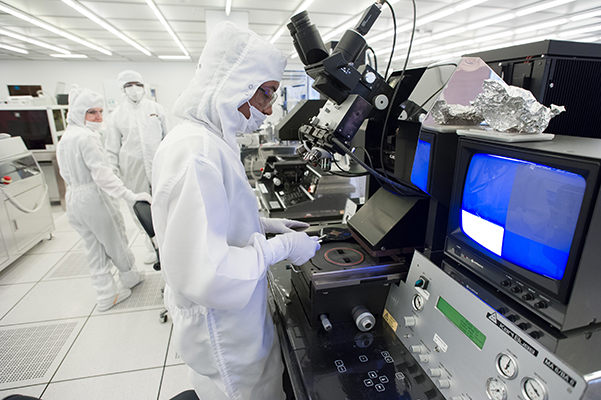
Researchers working in a semiconductor cleanroom at Georgia Tech. (Photo courtesy Christopher McKenney and Rob Felt)
Building a Bigger, Better Workforce
To take advantage of these new technologies, a workforce that knows how to build and use these chips is vital. “What we need today are more generalists who can work across the stack,” said Tom Conte, associate dean for Research in computing and professor in both computer science and electrical and computer engineering. “If we seize the opportunity to train people who can think across the layers of the stack, we can really innovate.”
Georgia Tech is also a crucial part of such training. With 28,500 square feet of academic cleanroom space—one of the largest in the nation—open to faculty, students, and outside researchers in industry, everyone can get hands-on experience in all parts of chip fabrication. “Our facility sees about a thousand users every year,” Filler said. “We are training people on the same types of tools that they would use in the semiconductor industry.”
ECE is collaborating with industry leaders to ensure the curriculum aligns with what semiconductor research requires. “CHIPS is adding momentum to society,” Raychowdhury said. “The companies have realized that the workforce gap needs to be addressed. Now that many of these companies have received CHIPS funding, more students are interested in semiconductors, and they want to learn and work for these companies.”
Building up the talent pipeline is also a strategy for the Institute, from expanding who does research to growing the workforce. Georgia Tech is collaborating with historically Black colleges and universities (HBCUs) and minority-serving institutions (MSIs) to build research partnerships and work on joint semiconductor projects that will bring more students into the field. “We need Clark Atlanta University, Morehouse College, and Spelman College— nd we need the communities those schools serve,” White said.
To this end, Georgia Tech launched the Research Collaboration Initiative (RCI) to develop these partnerships. The RCI kicked off with a research collaboration forum inviting HBCU representatives from across the nation in 2023, from which 17 grants were awarded. This group of 20-plus HBCUs conducts semiconductor research, while also engaging their local community colleges and K-12 schools in these efforts.
The talent pipeline for MSIs starts in K-12 and extends to two-year technical schools—and Georgia Tech is reaching out to everyone. “We need to embrace these students and show them that this industry offers a viable career path,” White said. One example of such early engagement is Chip Camp, a three-day STEM camp sponsored by Micron that offers sixth through eighth graders the opportunity to learn about the chip fabrication process and to see how a cleanroom works.
Investing in the Future
Georgia Tech’s objectives to improve semiconductor chips and build the workforce align with those of CHIPS.
“The CHIPS program will develop a unique collaboration ecosystem between federal and state governments, industry, national labs, and academia,” Bakir said. “Georgia Tech has a long history of partnering with these organizations; we look forward to continuing this partnership to explore a research agenda that meets the national needs for semiconductors and advanced packaging.”
Georgia Tech’s efforts in industry, education, and research in the race to create better semiconductors will help power the future.
“This is a pivotal moment for industry and education,” Lin said. “It signals a renewed investment in the engineers and researchers who will lead us into the next era of technological achievement.”
Tess Malone is a writer for Georgia Tech Research.
This article was originally published in Georgia Tech Research News.
Source: